
View a design
Open any revision of a project in the browser and review it without KiCad: browse the schematic, the board and the 3D model, follow a part or a net between them, and measure the board.
- Open the project from the workspace.
- Select Visualizers in the project sidebar.
- Pick a tab: Schematic, PCB, 3D, BOM, Stackup or
Assembly Assistant. The keys
1to6switch between them in that order.
The Visualizers show the branch or commit selected in the project header. To look at an older revision, open it from History (see Import and organize projects).
The first time anyone opens a revision, Prism may show Preparing design data… while it reads the files. See Design data for what that means and what to do if it fails.
Navigate the schematic
Section titled “Navigate the schematic”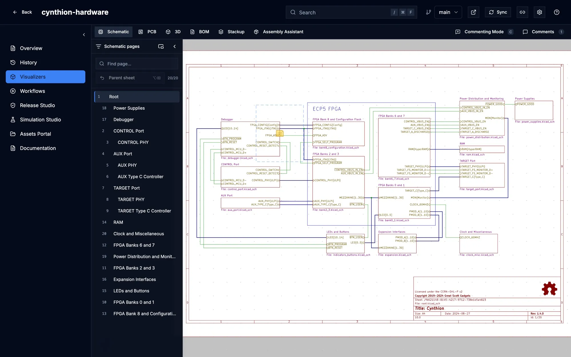
The Schematic pages panel on the left lists every sheet in hierarchy order.
- Click a sheet to open it, or type in Find page… to filter the list.
[and]go to the previous and next sheet.- Parent sheet, or
Alt+Backspace, goes up one level. - Drag the panel’s edge to resize it; the arrow at its top collapses it.
Change what the board shows
Section titled “Change what the board shows”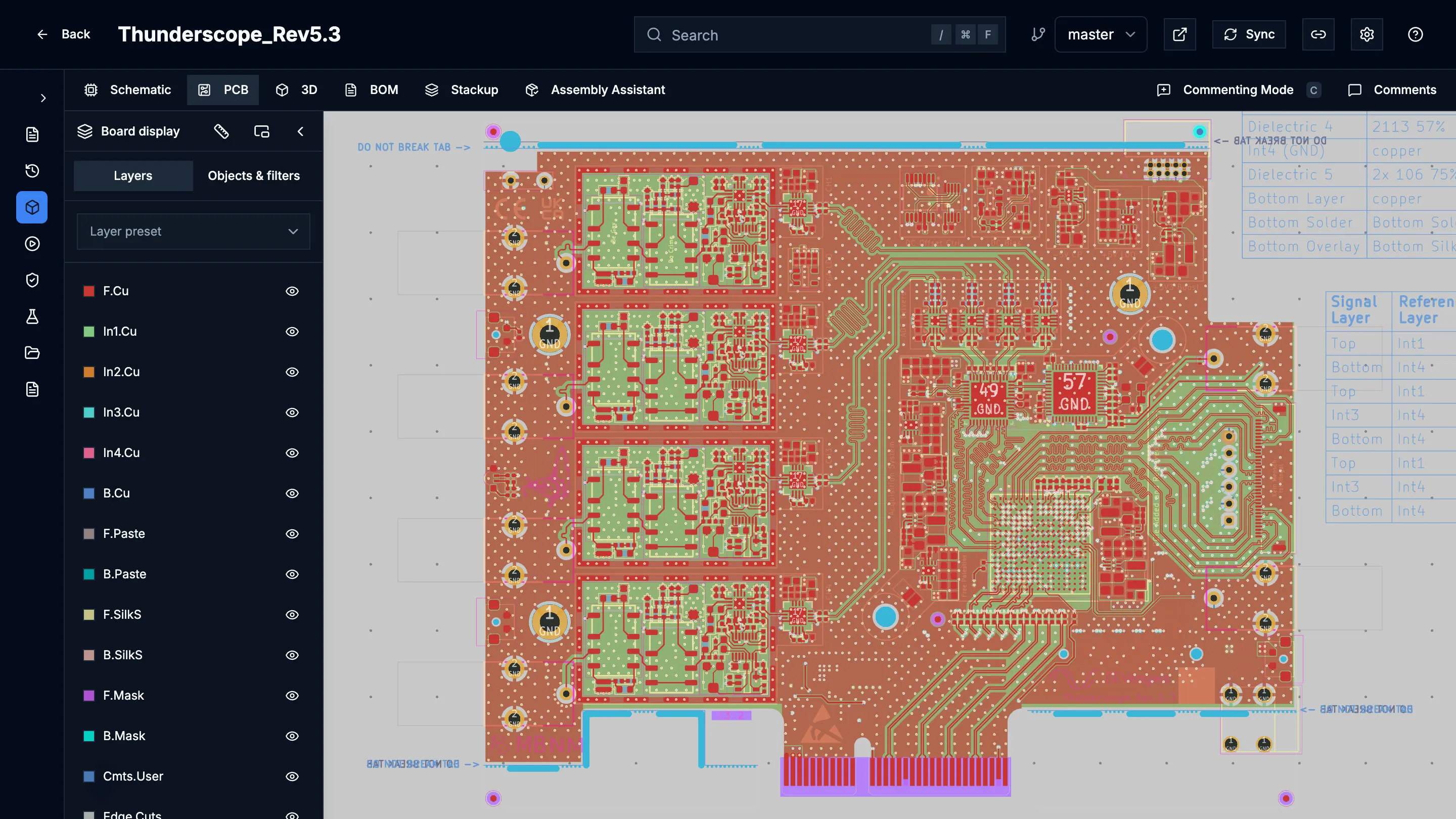
The Board display panel on the left of the PCB tab has two parts.
Layers
- Layer preset switches to a set of layers: Front, Back, All copper, Outer copper, Inner copper, Drawings, Show all or Hide all.
- The eye icon next to each layer shows or hides it. Click a layer’s name to bring it to the front.
Objects & filters
- Object opacity sliders for Tracks, Vias, Pads and Zones.
- Visibility filters for References, Values, Footprint text, Hidden text, Pad numbers, Net names on pads and Net names on tracks & vias.
- Highlight connected track emphasizes the copper connected to what you select.
Net names drawn inside filled zones are not shown.
Find a part or a net
Section titled “Find a part or a net”The search box in the project header searches the open design by reference, value, footprint or net name.
- Press
/or⌘F(Ctrl+Fon Windows and Linux), or click the box. - Type part of a name. Results are grouped under Components and Nets.
- Pick a result to select it, in this view and the others.
⌘K (Ctrl+K) opens the command palette instead, which searches projects,
views and actions across Prism. ? lists every keyboard shortcut.
Inspect a selection and cross-probe
Section titled “Inspect a selection and cross-probe”Click a symbol, footprint, pin, pad, wire or track to select it. The Selection panel on the right shows what it is:
- Component data: value, footprint, DNP and BOM flags, and the other fields of the part.
- Routing (PCB, nets only): routed length, layers used, and the number of tracks and vias.
- Connectivity: the net, its net class and the pin and pad it joins.
- Identity: references and identifiers, collapsed by default.
Selecting a part or a net also selects it in the other views: a symbol selected in the schematic is selected on the board and in the BOM, and the other way round. When you select a net or a global label, Instances lists every place it appears, with arrows to step through them, including other labels on the same sheet.
Press Esc, or select Clear at the bottom of the panel, to clear the
selection.
Highlight several nets
Section titled “Highlight several nets”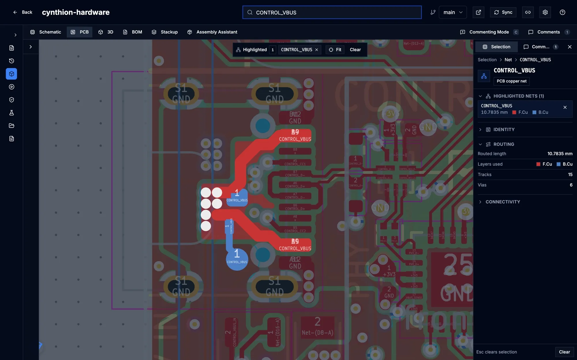
Shift-click a pin, pad, wire or track to add its net to the highlighted set. Shift-click it again to remove it.
- The Highlighted bar at the top of the canvas lists the nets. The ×
on a net removes it, Fit (PCB) frames all of them, and Clear (or
Esc) empties the set. - In the Selection panel, Highlighted nets lists each net with its routed length and copper layers on the PCB tab. Click a net there to inspect it.
- The highlighted set carries over between the Schematic, PCB and 3D tabs, and stays when you zoom.
A net with no copper on the board shows No copper on this board.
Measure on the board
Section titled “Measure on the board”On the PCB tab:
- Select the ruler icon (Measure) in the Board display panel, or
press
⌘⇧M(Ctrl+Shift+M). - Click two points. Points snap to the nearest object; hold
Shiftto place a free point. - Read the distance in the bar at the bottom of the canvas, and switch
between
mmandmilthere.
Esc clears the points, and a second Esc leaves measure mode.
Open insets
Section titled “Open insets”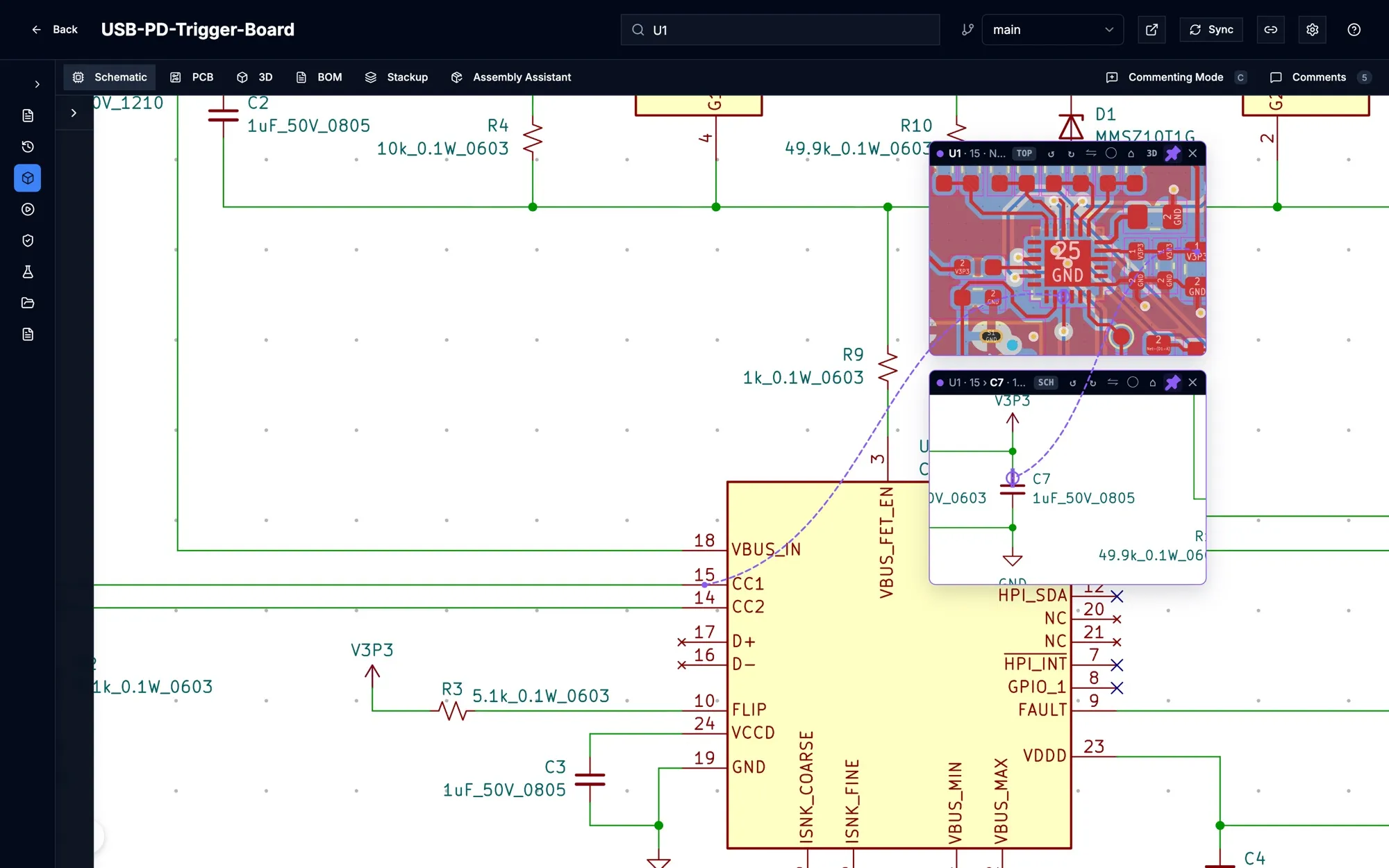
An inset is a small live view of the other document, opened from the one you are reading: hover a schematic pin to see the board around its pad, or hover a PCB pad to see the schematic around its pin. A dashed line joins the pin or pad to its counterpart in the inset.
- Turn on inset mode: press
Ior select the Insets button in the left panel of the Schematic or PCB tab. With inset mode off, holdAlt(⌥on macOS) to peek, and release it to close the peek. - Hover a pin or pad. A preview opens with a dashed border and closes when you move away, unless the pointer is over it.
- Click the pin or pad to pin its inset. A pinned inset stays until you close it.
- Hover a pin or pad inside an inset to open the next document from there. Insets chain (schematic → PCB → schematic …), and each one names its parent in its header. Closing an inset also closes the insets opened from it.
Drag an inset’s header to move it, its corner to resize it, and its canvas to pan; the mouse wheel zooms. A footprint on the bottom side opens mirrored with a BOT badge. Insets follow the main view: layer visibility, highlighted nets, the selection and the design variant all apply to them.
With the pointer over an inset:
| Key | Action |
|---|---|
R / ⇧R |
Rotate +15° / −15° (⇧ + wheel rotates freely) |
M |
Mirror |
L |
Lens (circular) shape |
Home |
Refit |
P |
Pin or unpin |
T |
Show the board in 3D (PCB insets) |
X |
Close |
Esc |
Close the preview, then all insets |
At most eight insets stay open; opening another closes the one used least recently. Insets belong to their tab: switching tabs closes unpinned previews and keeps pinned insets. The first PCB inset on a large board can take a moment, because the board view loads the first time inset mode turns on.
Explore the board in 3D
Section titled “Explore the board in 3D”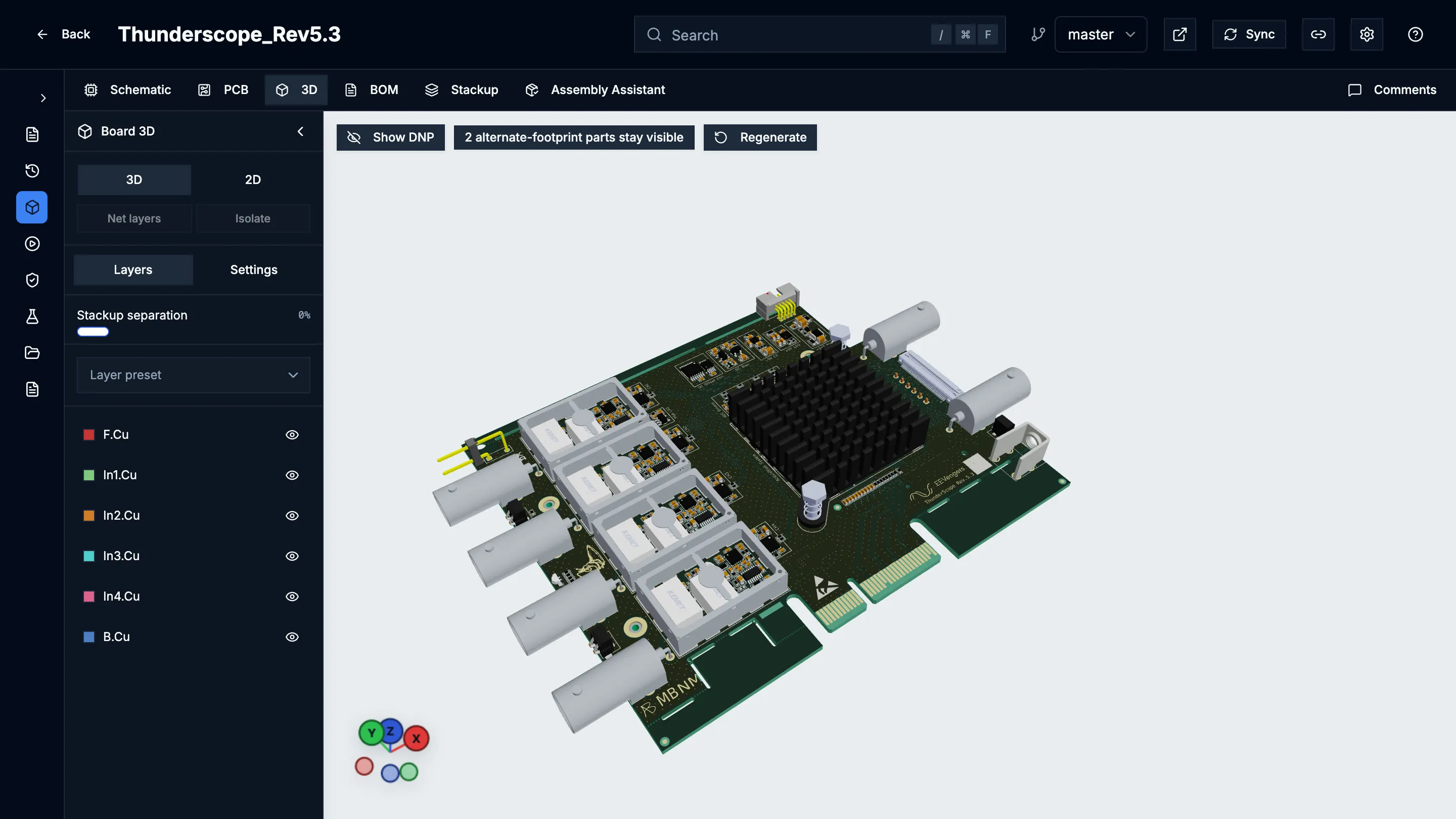
The 3D tab shows the assembled board. The bare board can appear before the parts; a badge at the top shows the loading stage until everything is in.
- Drag to orbit, and use the wheel to zoom.
- 3D and 2D switch between the model and a flat layer view.
- Layers has Stackup separation, to pull the layers apart, a Layer preset, and a visibility toggle per copper layer.
- Settings turns Board substrate, Components, Model placeholders and Realistic colours on or off.
- Right-click a part and choose Hide or Show only. Show all puts every part back.
- Show DNP shows the parts marked do-not-populate, which the 3D view hides by default.
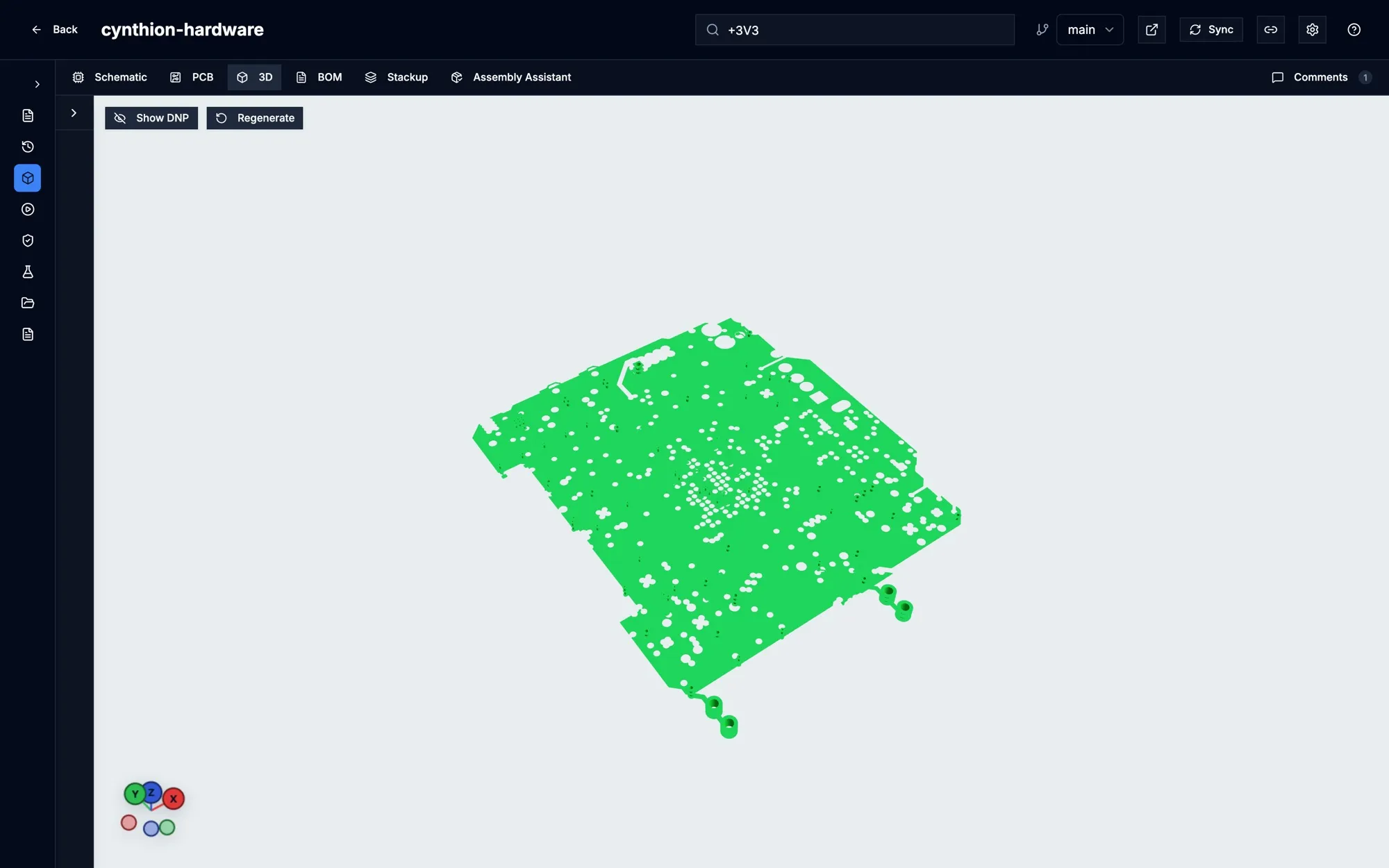
Highlighted nets are emphasized in 3D as well. With a net selected:
- Net layers shows only the layers that net uses.
- Isolate, or
I, hides everything except that net.
If a revision’s 3D model has not been built yet, the tab says so. A designer or admin can select Generate 3D assets, or Regenerate to rebuild it.
Other tabs
Section titled “Other tabs”- BOM and the Variant menu are covered in Variants and BOM.
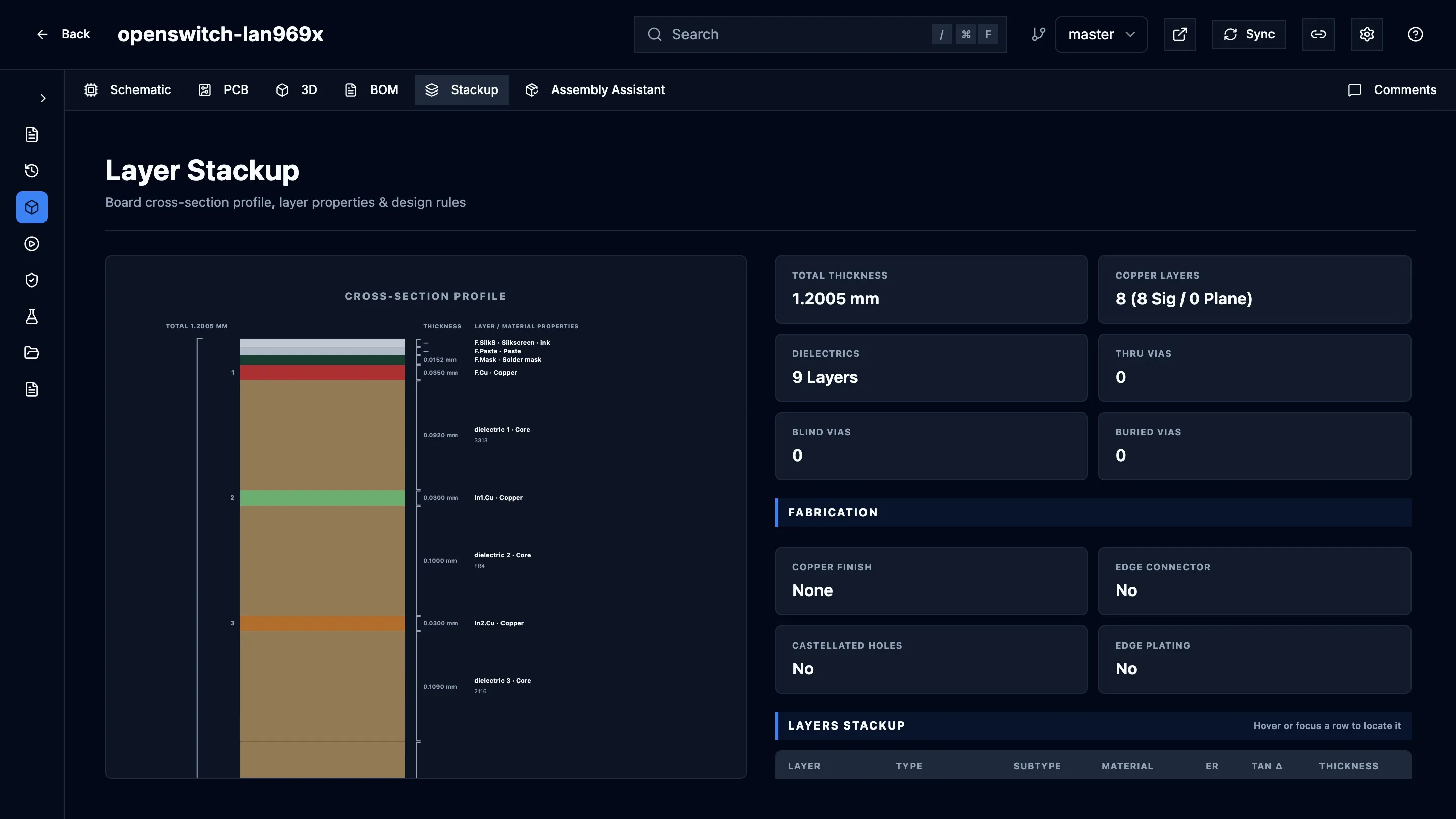
- Stackup shows the board’s layer stack, fabrication properties and design rules.
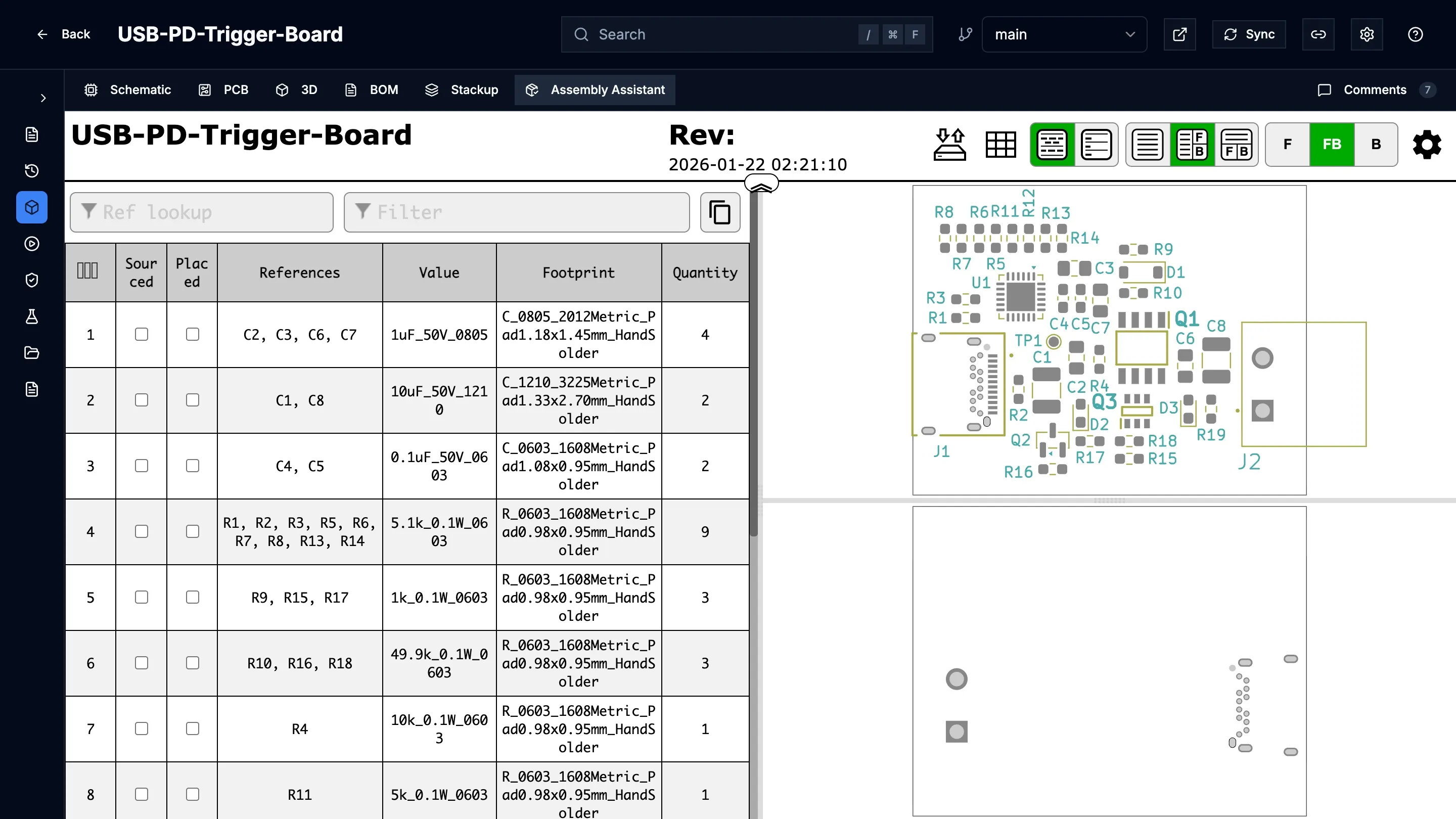
- Assembly Assistant shows the interactive HTML BOM generated for the revision, if the project has one.
Share what you are looking at
Section titled “Share what you are looking at”The URL of a Visualizers page records the open tab, the selected parts, the highlighted nets, the schematic sheet and the framed region. Copy it from the address bar to send someone the same view; open a commit first if the link must keep pointing at one revision. See Links to a view.